Analog Current Drive Amplifier — User Manual
Complete technical manual: pinout, protections, filter adjustment, specifications.
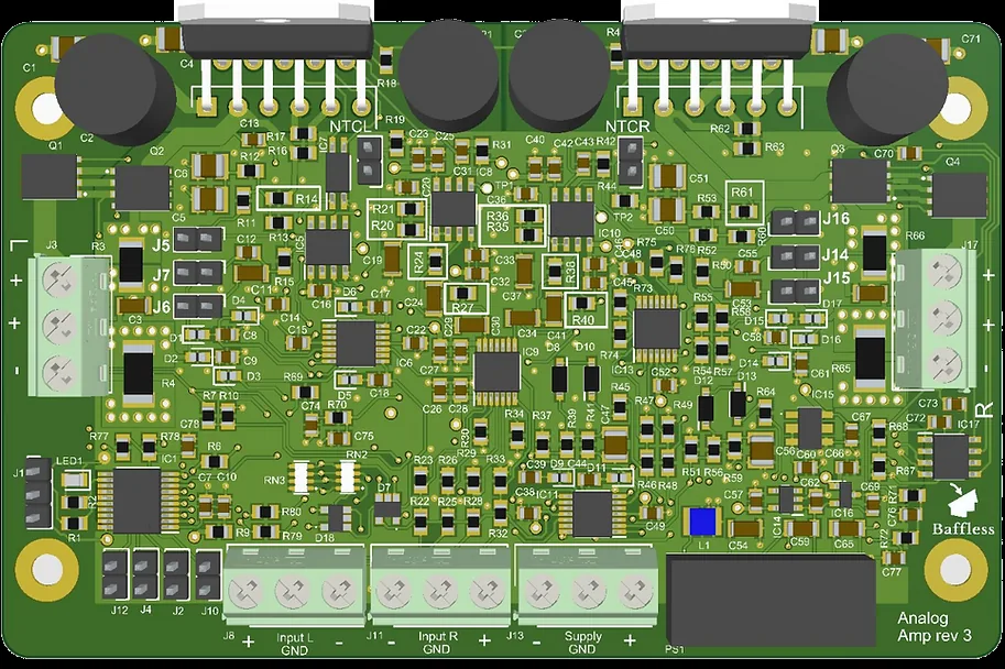
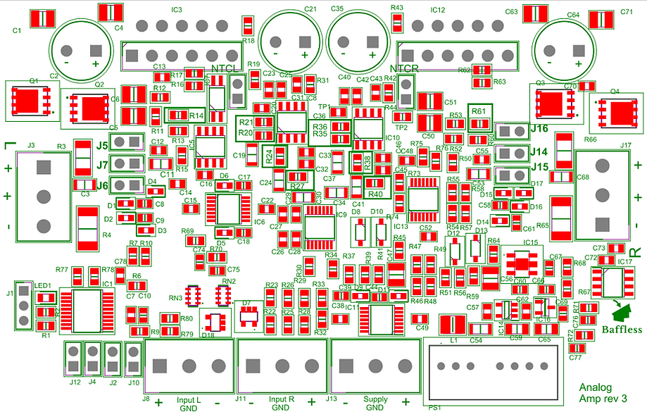
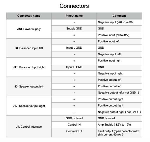
Pinout and layout
Powering on
Amplifier power on/off is controlled by the external power source. Turn on the power supply and the amp will silently power on. If the amplifier is powered and no errors exist, the green LED will be on.
Fault output
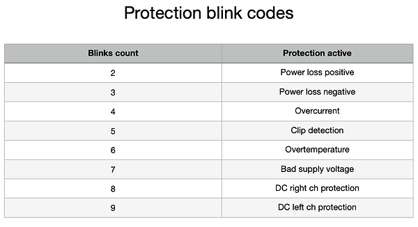
The amplifier can output faults on the green LED as a blink code: a pause, then a counted number of blinks.
Amplifier protections
The amplifier has these protections:
- Overtemperature protection
- Clip protection
- Overcurrent protection
- DC protection
All of these report their state on the green LED. If a protection is active, the LED blinks a 500 ms pulse every second, followed by a 2 second pause. Counting the blinks tells you which protection is active.
When a protection kicks in, the amplifier goes off and stays off until reset. Reset by repowering from the power supply. Blink codes are shown above.
- Clip protection is more a quality feature than a safety feature. If clip is detected, the amp mutes for 3 seconds and tells you to lower the input. If that happens more than 5 times in 30 seconds, the amp switches off, the blink code appears, and a reset is needed. The point is to warn you that you are entering the clip zone and the input has to be reduced.
- Power loss protection is the silent turn on/off feature. It can also detect a short voltage drop on the rails. If the drop is more than 4.5 V but the voltage stays above about 20 V, the amp switches off and blinks the error code.
- Overcurrent protection kicks in above 5.4 A. Reaction time is 30 µs.
- Overtemperature protection uses a thermistor on the power chips, set at 75 °C. If the heatsink is not adequate or airflow is restricted, this protection switches the amp off. The blink code is shown.
- DC protection. If DC is present on the output, the amp switches off. It activates around 100 mV.
- Bad supply voltage is checked only at startup. If one rail is missing or the voltage is outside 20–40 V, the amp will not start. It does not protect the amp from damage if more than 42 V is supplied or reverse polarity supplied.
There is a second layer of overcurrent and overtemperature protection on the LM3886 power chip itself, at higher current and temperature.
Speaker outputs
Speaker output terminals J3 and J17 have two + pins. They are internally connected. The − pins are not grounded and must not be grounded in any way. Both speaker terminals must be left floating. Channels cannot be paralleled or bridged left with right. The − pin also carries some voltage, so it is tricky to measure amplifier performance accurately if you want to do so.
Stability
This amp is not inherently stable with all loads. In other words it is not unity-gain stable. It is stable with resistive loads of 3.3 Ω and more. Below 3.3 Ω, oscillations can start. That is only with a resistive load, and in current mode.
Lower resistance reduces the effective gain of the current amp, phase margin drops, and the amp can oscillate. With a real electrodynamic driver the inductance isolates the resistive part, so this is not a real problem in practice.
Even on a resistive load, if oscillations start they rise until overcurrent protection kicks in. You can test that by shorting the outputs in current-drive mode: the amp switches off and a blink code appears.
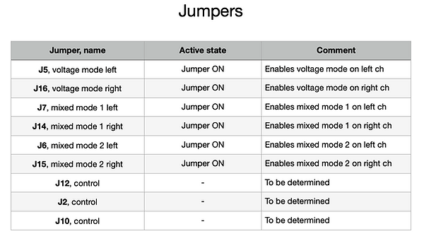
Jumper configuration
Frontend filter (for advanced users)
This section is for an advanced DIYer. It requires electronics knowledge.
Input sensitivity
Input sensitivity (Pic. 7) can be decreased from the default if needed. R26, R23, R33 and R29 can be reduced to form a divider. For example, 10 kΩ resistors there lower sensitivity by about 6 dB.
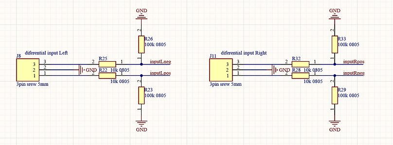
Pic. 7 Input sensitivity
EQ filter adjustment
EQ filter adjustments are also done by soldering resistors. By design they must stay strictly between the min and max values in Table 1. If you do not understand the idea, or want to do the filter in DSP, skip the rest of this section. If you know what you are doing, here is a TINA-TI design file for filter response calculation: filter part.zip.
In mixed mode 1 this filter can adjust response to within 1 dB of voltage-mode response. Overall adjustment is better in DSP. The best option is to lower the high-frequency boost with the first and second cut filters on this analog filter, and do the resonance-bump EQ in DSP. That improves the SNR of the amp. Two RC filters in series create the desired slope.
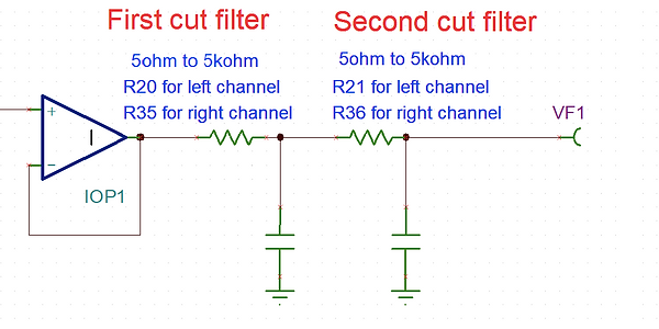
The most awkward part of current drive is that output rises at resonance. In reality the SPL peak is a lot lower than the driver’s impedance graph suggests. In mixed mode the output impedance is already fairly low at resonance, so the SPL peak stays low. A simple filter fixes what remains.
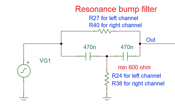
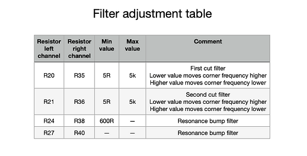
Table 1. Filter adjustment table
Output impedance
The amplifier has 3 modes of operation:
- Voltage
- Mixed mode 1
- Mixed mode 2
Output impedance is 0.5 Ω in voltage mode. If you really need it, it can be reduced to about 0 Ω by disconnecting the speaker negative return from J3/J17 minus and connecting it to J13 Supply GND instead. Warning: you then lose overcurrent/oscillation protection, and the amp will work only in voltage mode.
Mode 1 and mode 2 change impedance with frequency (Pic. 8). Mode 2 is more of a current drive, at the expense of higher output impedance at the driver’s resonance. If output impedance is more than 10 times the load impedance — around 100 Ω — it can be considered current drive. Above that it is nice to have, but it makes less and less difference.
- Mixed mode 1 is probably the preferred way if you are working at the driver’s resonance.
- Mixed mode 2 is more of a current drive and can be the favourite in a multi-channel system working above resonance, where the peak is not a concern.
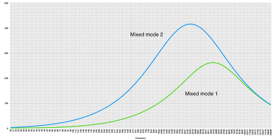
Pic. 8 Mixed mode impedances
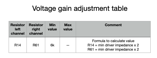
If the amp is used in mixed mode without DSP, resistors R14 and R61 may need to change. It depends on the connected driver’s minimum impedance. Find that minimum and multiply by 2. Gain in current mode depends on driver impedance, so the voltage-to-current transition has to be matched if you want a flat response. See Pic. 9.
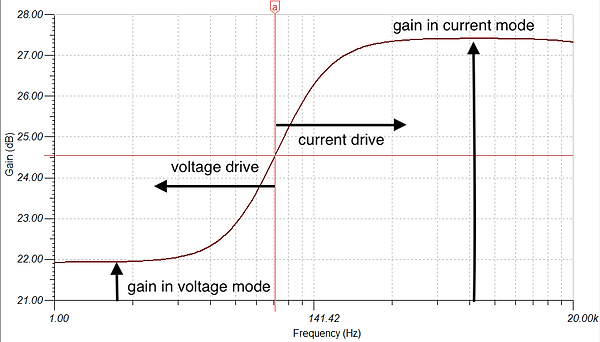
Pic. 9 Mixed mode gains
Power supply and heatsink
The board is designed for an SMPS supply and works best with one. A transformer-based supply is not recommended: voltage variation can cause issues, some protections may need disabling, and usable power output will be reduced. SMPS does not degrade sound quality if the amp is done right. A CONNEX SMPS300REh will work well. ±36 V looks optimal if you have no other constraints: lower voltage limits output capability, higher voltage increases idle heat. It depends on the application.
Heatsink also depends on the application. 0.4 °C/W is nice to have. Something like the Dissipante 3U 300mm used in this enclosure.
Dimensions
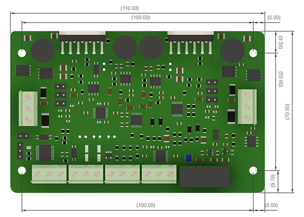
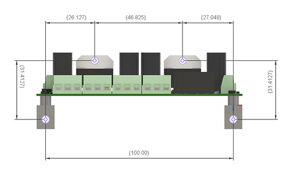
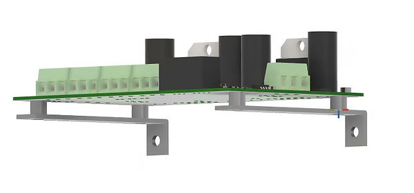
Dimensions are in mm. The bottom picture shows four holes to mount the amplifier to a heatsink. The amplifier comes with L-shape brackets. M3 bolts can be used.
Do not overtorque! 0.5–0.6 Nm (4.5–5 lb-in) for M3 bolts.
Specifications
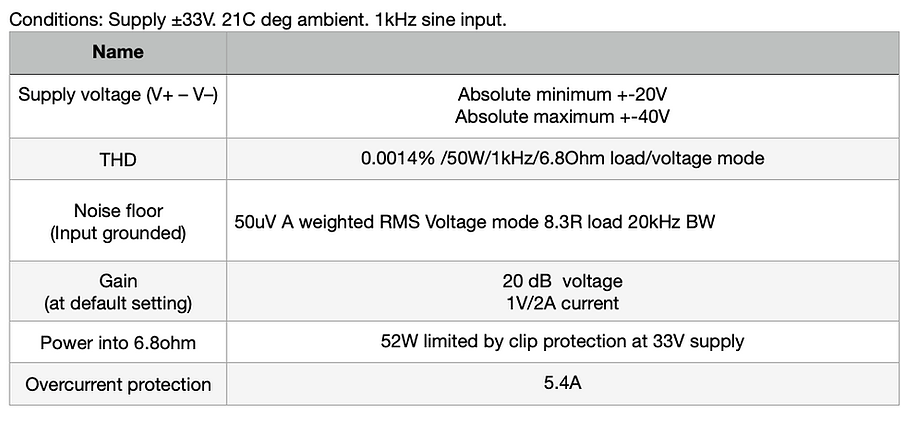
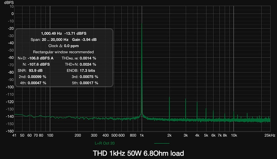
THD at 1 kHz, 50 W, 6.8 Ω load